Our research focuses on building, developing, and characterizing nano-photonic devices and quantum materials including 2D materials, semiconductor quantum dots, and hybrid quantum systems that are relevant for applications in quantum science and technology.
-
Strain tunable quantum emission
Strain engineering is a natural route to control the electronic and optical properties of two-dimensional (2D) materials. Strain engineering is not only responsible for the activation of quantum light emission in 2D materials but can also be used to dynamically tune their photophysical properties. We are interested in understanding the effects of static and dynamic strain tuning of localized emitters in monolayer crystals as well as van der Waals heterostructure.
Chakraborty et al, Optica 7, 6 (2020) -

Integrated Nanophotonics
Efficient coupling of qubits with one another as well as photonic devices forms the basis of many essential functions of a quantum network. Coupling quantum emitters with optical cavities will enhance their light extraction efficiencies and the performance of recently demonstrated waveguide coupled emitters.
Peyskens, Chakraborty et al, Nature Comm. 10, 4435 (2019)
-

2D excitonics
Valley contrasting polarization selection rules present unique opportunities for optical control in valleytronic devices. We are interested in exploring the effects of mechanical strain and electric field on the valley polarization and valley dynamics in 2D excitons.
Chakraborty et al, Opt. Mater. Exp. 9, 3 (2019) -
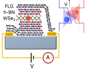
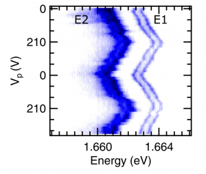
Voltage Controlled van der Waals heterostructure
Control and manipulation of a single charge and its internal degrees of freedom are critical for quantum science. Charge carriers in TMDCs possess an optically addressable valley degree of freedom, which is locked to their spin in presence of large spin-orbit coupling. A natural question for quantum information science and quantum metrology applications is whether a single spin-valley qubit can be optically addressed and manipulated. Charge tunable van der Waals heterostructure can be used to localize single electron and hole in 2D quantum emitters and dynamically tune their emission properties.
Chakraborty et al, Nature Nano., 10, 6 (2015). Chakraborty et al, Nano. Lett, 17, 4 (2017). Chakraborty et al, Nano Letters, 18, 5 (2018) -

Atomic defects for quantum technology
Atomic defects in materials possess quantum degrees of freedom that can form qubits for quantum technologies. Designer quantum defects with favorable optical properties can be predicted using ab-initio simulations. Some of the guiding criteria include material bandgap, spin-orbit coupling, electron-phonon interactions, nuclear spin concentrations, and crystal symmetry.
Chakraborty, Ciccarino et al, arXiv:2007.14399 (2020)