Facilities
University Center Facility
- University of Delaware Nanofabrication Facility: state-of-the-art clean room facility.
- Keck Center for Advaced Miscroscopy and Microanalysis: TEM, Focus Ion Beam (FIB), SEM, etc.
- Advance Materials Characterization Lab: Variety of instrument for material characterization.
Material Fabrication
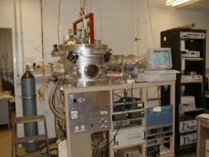
Magnetron Sputtering System
- Multiple gas environment: Ar, N2, O2, NH3
- Multiple sputtering guns (cathodes): 7 in each systems with RF and DC power
- plasmon oxidation gun for fabrication of Al2O3 and MgO tunnel barrier
- Substrate rotation: rotation around the center and self rotation
- Substrate temperature control: 77 K to 800 K

Vacuum Annealing in Magnetic Field
Spin-spray Ferrite Deposition
Fabrication of Ferrite films at low temperature

Precursor solution flow rate: 0.06-2300 ml/min
Substrate heating: 200 C
Substrate rotation: 100-1500rpm
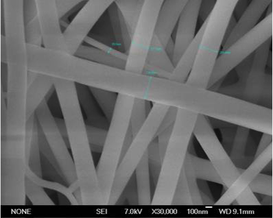
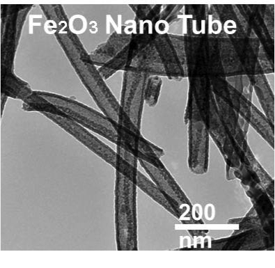
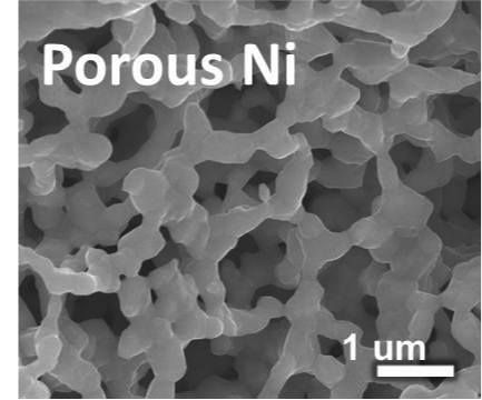
Fabrication of nanofiber, nanotube, and porous materials
Materials: polymers, metals, oxides, and compounds

 |
 |
 |
 |
Electrochemical Deposition
 |
 |
 |
Computer-controlled Potentiostat/Galvanostat 100 V compliance, 2 A current output
•Potentiostatic •Potentiodynamic •Cyclic Voltammogram •Potential Square-Wave •Potential Stair-Step •Potential Scan/Hold •Polarization Resistance •Square-Wave Voltammetry •Galvanostatic •Galvanodynamic •Galvanic Square-Wave •Galvanic Cycle •E&I Noise
CVD for Graphene Fabrication

Annealing Furnace
Four furnaces offer temperatures as high as 1500 C, with a choice of ambient environment, N2, forming gas (H2 5%+Ar 95%), O2, and Ar.
Material Characterization
Rigaku Ultima IV X-Ray Diffractometer.

Vibrating Sample Magnetometer (VSM)
Lakeshore VSM
Films and Powder Samples

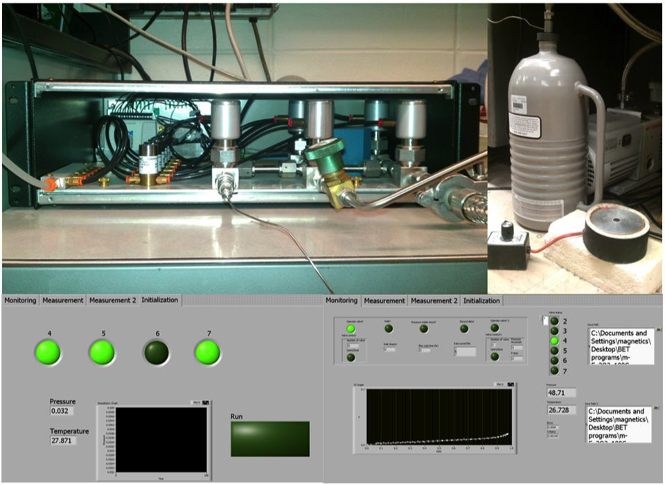
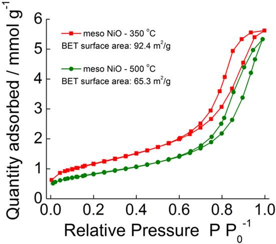
BET Surface Area Measurement
Surface Area: BET Theory
Pore Distribution: BJH Method
Minimum Surface Area: 0.2m2
 |
 |
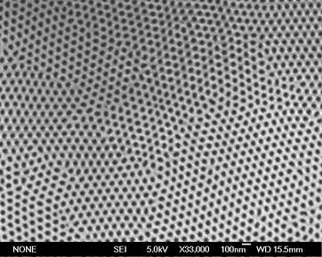
Field emission microscopy
EDS Detector
Phase contrast microscopy

Dynamic Light Scattering (DLS): Melvern Zetasizer

Size: 0.3 nm to 0.01 mm
Zeta potential: 3.8 nm to 0.1 mm
Molecular Weight: 980 Da-20M Da
TemperatureL 0-90 °C
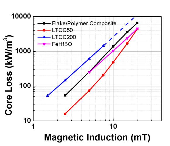
Hysteresis loop measure of soft magnetic materials: coercivity and power loss
Frequency: 50Hz to 1MHz
 |
 |
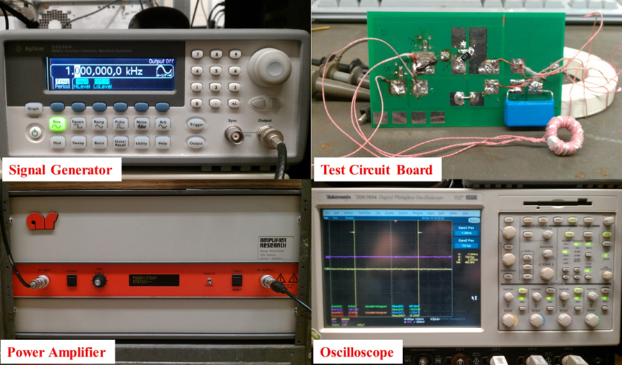
High Frequency & High Power Inductor Power Meter
 |
 |
Power loss measurement of soft magnetic materials
Frequency up to 20 MHz
 LCR meter with magnetic test fixture |
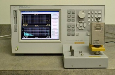 LCR Meter with dielectric test fixture |
 |
L, C, R Measurements up to 1GHz
Complex permeability and permittivity spectrum up to 1GHz
Microwave Characterization Suite
Microwave probe station, 7mm coaxial airline fixture, resonators, waveguides, and antennas
FMR Spectroscopy
Spinwave propagation spectroscopy
Spin Torque Transfer -FMR
Permeability and permittivity spectra
 HP8722ES VNA |
 Agilent N5230C PNA |
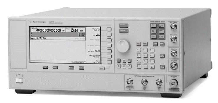 Agilent E857 PSG Signal Generator |
Magneto-Optical Kerr Rotation (MOKE)
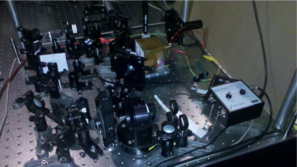
Scanning longitudinal and Polar MOKE
Combined with spintronic measurements fir current-driven spin obrit torque measurement
Electrical Transport Measurements
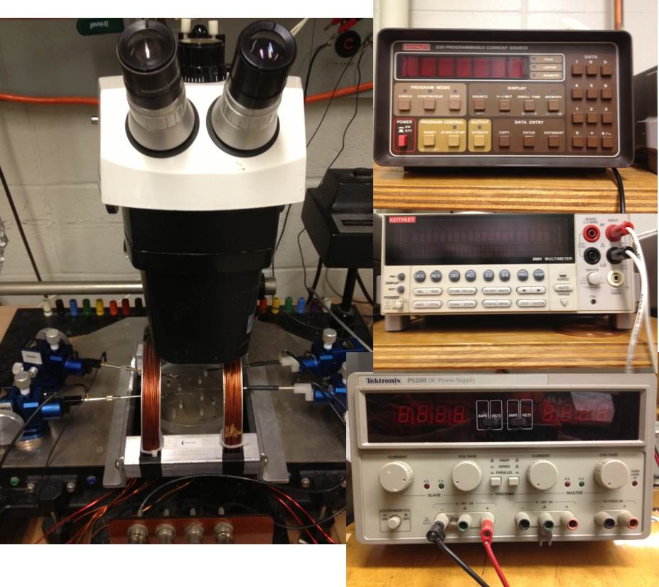
Resistivity
I-V Curve
Impedance spectra up to 100MHz
Thermal Transport Measurements

Spin Seebeck Effect
Nernst Effect